
It’s been almost four years since the world entered the era of artificial intelligence popularized by natural language processing tools with the public release of ChatGPT. In those four years, AI has made plenty of headlines — for better and for worse — while OpenAI and its competitors have used the time to improve the technology. Two years ago, I had some fun programming a Tetris with AI, with mixed results. But that experiment confirmed what I suspected: AI is a very good doer, but its results depend above all on the prompts it’s given. That hasn’t stopped vibe coding from becoming trendy: even Linus Torvalds has gotten into it… carefully! One thing led to another — and with no smooth segue, I admit! — old Bob decided to vibe-code an emulator! Why? Simply because I’ve been a heavy user of these little magic programs for a good quarter of a century, and it annoys me not to understand how they work! After a quick think, I decided my emulator would target the NES, which has all the advantages for a project like this: the console is fairly simple, while its popularity means all its secrets have been uncovered, making it easy to find extremely complete documentation.
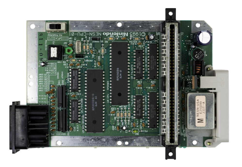
When I say I don’t understand how an emulator works, I’m abbreviating: the basic principle is dead simple! It’s about virtually reproducing, through pure programming, the behavior of the console’s electronic components so you can run the pre-dumped game program — that is, copied and placed into a standardized software container (the famous ROM of emulation). Going from principle to a working program is another story. That’s where ChatGPT (in my case!) comes in: I’m counting on it to write the code I need — and explain it to me! Otherwise, what’s the point of taking on this challenge? Quality NES emulators exist, and I’ll never do better. The important thing, as in life, isn’t the destination but the journey. With that mindset, I started my adventure in emulator land, only to quickly hit a first obstacle: it’s impossible to understand how to program the emulator without first understanding how the NES itself works!
There’s no shortage of documentation and articles on this legend of video game history. Whether it’s an exhaustive presentation of the NES electronics and how it works or a game that challenges you to code a NES emulator interactively, the Internet is full of resources. Almost too many, really: the Bible of NES programming (nesdev.org) is ultra-complete but also ultra-dry, and pulling together all the useful information into a coherent whole can be time-consuming and discouraging… What if, in addition to being a good doer, ChatGPT could be a good teacher? From idea to execution is just one step: with a few well-constructed prompts and a few iterations, I was able to build the NES understanding course I needed! Let’s be clear: AI doesn’t invent anything and is definitely not a teacher-researcher. But it’s an excellent secretary that gathers, synthesizes, and formats large amounts of information in no time!
And that’s the genesis of the little “Manual for Understanding the Nintendo NES/Famicom” I’m offering you today. A slightly long genesis, I admit; but necessary: this is my site, mine alone, yet what you’re about to read wasn’t written by Bob but by ChatGPT (with some corrections, tweaks, and edits nonetheless). So I had to include a bit of human writing, at the risk of sounding like a charlatan!
Bob Dupneu
MANUAL FOR UNDERSTANDING THE NINTENDO NES/FAMICOM
A game is a program accompanied by data. The console executes this program, reads the player’s inputs, and drives specialized circuits to produce picture and sound. The cartridge — or any other medium like a disk — provides the necessary information.
The Family Computer, commonly called the Famicom, appeared in Japan in 1983. Its architecture was adapted for other markets under the name Nintendo Entertainment System, or NES, starting in 1985. These machines belong to the same family, but their connectors, frequencies, and certain compatibility mechanisms differ.
We’ll start from the simplest notions, then follow the path of the data to the screen. Technical terms link to the glossary at the bottom of the page, and “For more” notes link to the useful resources. Unless otherwise noted, descriptions refer to consumer models and their usual operation.
Table of contents
- The console and its main circuits
- Bits, bytes, and the CPU
- Addresses, buses, and memory
- Cartridges and mappers
- How the image is made
- Controllers and sound
- From startup to the game loop
- Regional differences
- The 10NES/CIC lockout
- The Famicom Disk System
- Media and their evolution
- What changes with “16-bit”
- Game files and emulation
- Key takeaways
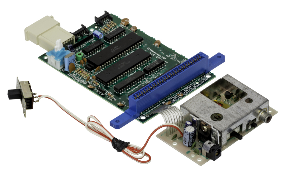
1- The console and its main circuits
An NES cartridge doesn’t contain a prerecorded video. It contains, among other things, instructions, level descriptions, graphic patterns, and music data. At every moment, the console builds the result that corresponds to the game’s current situation.
Four elements share most of the work:
- The CPU, or central processor, executes the program: movement, collisions, enemies, score, game rules, and interpreting inputs.
- The PPU, or graphics chip, builds the image from small patterns, background tile maps, palettes, and graphical objects called sprites.
- The APU, or sound chip, produces audio based on parameters set by the program.
- The cartridge provides memory and, often, additional logic. It genuinely participates in how the machine operates.
The circuits work in parallel. While the PPU builds an image and the APU produces sound, the CPU can compute the next game state. These are not four steps executed strictly one after another.
For more: general architecture overview.
2- Bits, bytes, and the CPU: the basics
One bit represents two possibilities
A bit can take two values: 0 or 1. You can picture it as a switch off or on. In circuits, these values are electrical states, not tiny mechanical switches.
One bit is enough, for example, to represent “button released” or “button pressed.” To express more possibilities, we group several bits.
Eight bits form a byte
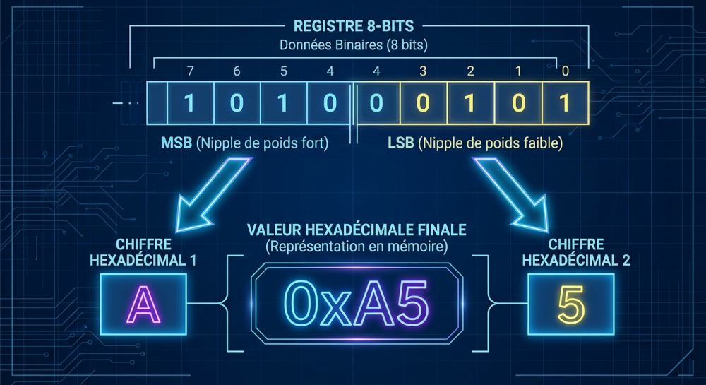
Each added bit doubles the number of combinations: two bits give 4, three bits give 8, and eight bits give 28 = 256. A byte can therefore represent an integer from 0 to 255.
In binary notation, positions are worth 1, 2, 4, 8, 16, 32, 64, and 128 from right to left:
Position value:           128  64  32  16   8   4   2   1
Bit:                        0   0   0   0   1   1   0   1

Represented value: 8 + 4 + 1 = 13
But a byte isn’t necessarily used as a number: it can describe buttons, a piece of an image, or an instruction. The program and hardware give meaning to bits.
Why is the NES called “8-bit”?
Its CPU is chiefly organized to manipulate data in eight-bit chunks. Its arithmetic unit works on values of that size, and its data bus transports eight bits at a time.
That does not mean “eight colors,” “256 memory slots,” nor “impossible to compute beyond 255.” To represent a large score or a position in a long level, the program can use multiple bytes.
Take 250 + 10 = 260. The result doesn’t fit in a single byte. An eight-bit addition then yields a result of 4 with a carry. The program carries this into a second byte:
Two bytes containing 1 and 4 can represent 1 × 256 + 4 = 260.
It’s the principle of “carry-over” addition from grade school, but with chunks of 256 values rather than decimal digits. A processor that can directly compute on sixteen bits can perform this addition more directly. We’ll revisit this comparison in the section on 16-bit consoles.
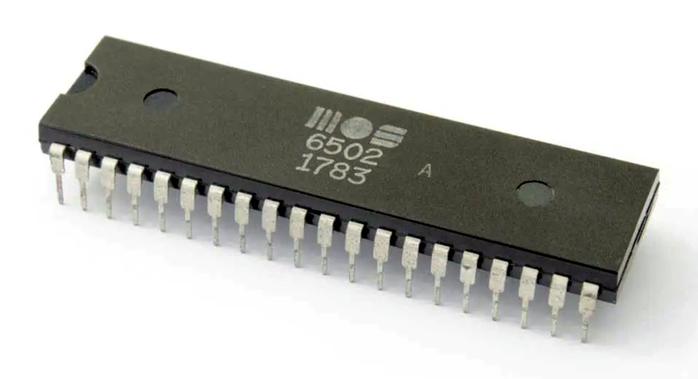
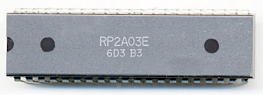
The compute core: a derivative of the MOS 6502
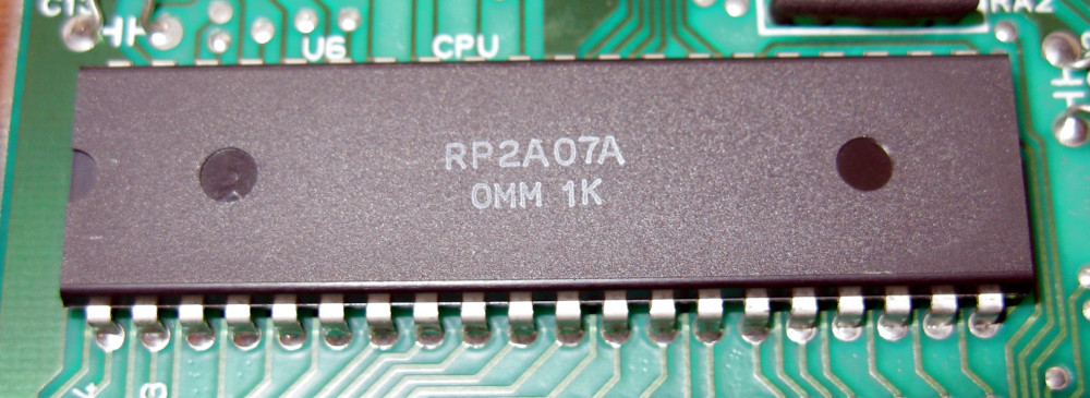
The main chip is a Ricoh 2A03 on the Famicom and NTSC NES units, or a Ricoh 2A07 on PAL NES. It combines notably the CPU, the APU, and logic for certain memory transfers.
The CPU derives from the MOS 6502, largely reusing its instruction set. An important difference is the absence of functional hardware decimal arithmetic BCD. That doesn’t prevent computing or displaying scores: the program performs the needed conversions.
MHz measure a clock rate, not an instruction count
An electronic clock paces the CPU’s work like a metronome. One megahertz, or MHz, corresponds to one million clock cycles per second.
- Famicom and NTSC NES: about 1.79 MHz.
- PAL NES: about 1.66 MHz.
An instruction generally requires several cycles: reading the bytes that describe it, possibly fetching a data value, performing an operation, etc. 1.79 MHz therefore does not mean 1.79 million completed instructions per second.
Machine code and assembly
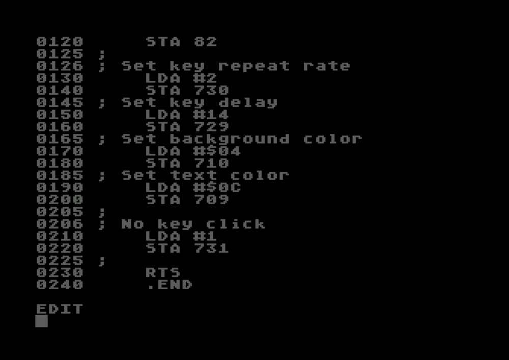
The CPU doesn’t understand a sentence like “make the character jump.” It executes elementary operations encoded in bytes: that’s machine code. Assembly provides a readable notation for those operations.
In a common assembly syntax:
LDA #13This instruction requests placing the value 13 into the CPU’s accumulator, a small working register. It translates to two bytes:
10101001  00001101
operation value 13
The CPU reads these bytes in sequence. An instruction can therefore take several bytes, even on an 8-bit processor.
For more: CPU and its memory map.
3- Addresses, buses, and memory
An address is not the content of its slot
Imagine memory like a cabinet filled with slots. Each slot has a number, its address, and can hold one byte.
Slot number 300 can contain the value 13. The number helps find the slot; it doesn’t describe its content. Similarly, a mailbox labeled 12,500 can contain a card that just says “3.”
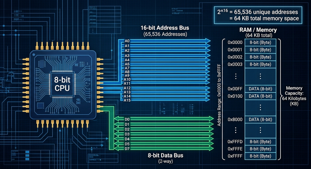
The NES CPU uses sixteen-bit addresses. It can therefore distinguish:
216 = 65,536 addresses, or a 64 KiB address space.
A KiB, or kibibyte, contains 1,024 bytes. Possible addresses go from 0 to 65,535.
Two buses of different widths
A bus is a set of electrical connections that carry information. The CPU notably has:
- a sixteen-bit address bus, indicating where to read or write;
- an eight-bit data bus, transporting the content read or written.
CPU ─── 16-bit address ───► Memory
              “slot 300”

CPU ◄── 8-bit data ─────── Memory
              “value 13”
There is thus no contradiction between “8-bit CPU” and “16-bit addresses.” These numbers describe different functions.
64 KiB of addresses doesn’t mean 64 KiB of RAM
The console includes notably the following memories:
- 2 KiB of work RAM for variables, positions, counters, and temporary data;
- 2 KiB of RAM for background maps, accessed in the PPU’s address space;
- 256 bytes of primary OAM, describing sprites;
- a small palette memory, exposed in a 32-byte area with mirrored addresses.
On top of that come the cartridge or Disk System memories. ROM retains its content without power and is normally not modified during play. RAM is writable, but it normally loses content once unpowered.
Addresses for memory… and to command circuits
Some addresses do not correspond to a RAM slot. They give access to hardware registers: control points or status readouts of circuits. Writing to an address can thus modify sound or display.
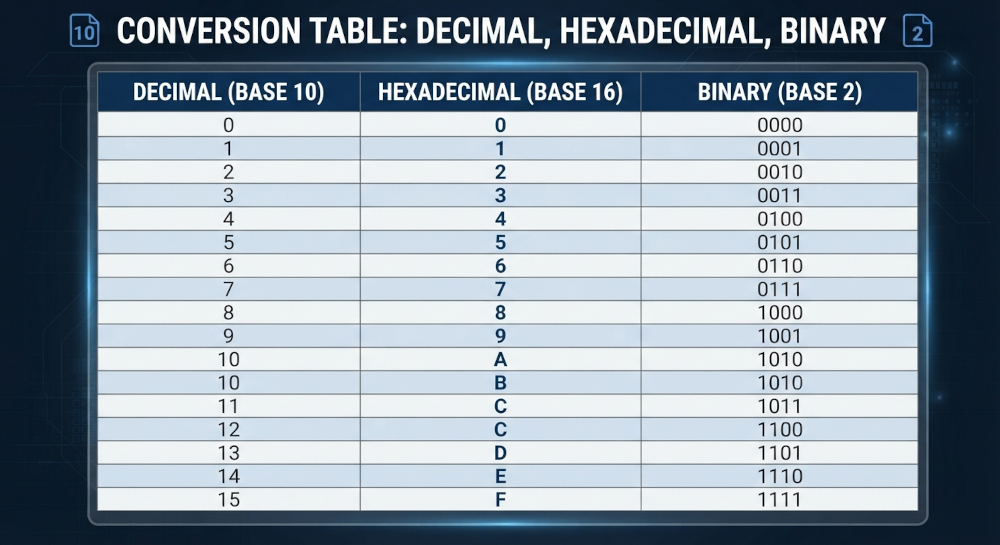
In the map below, the $ prefix indicates
hexadecimal notation (base sixteen).
For example, $FF equals 255.
| Addresses | Usual purpose |
|---|---|
$0000–$1FFF |
2 KiB of work RAM, visible four times due to address mirroring. |
$2000–$3FFF |
Eight PPU registers, also repeated across this range. |
$4000–$4017 |
Audio controls, controller reading, and sprite transfer command. |
$4020–$7FFF |
Area available for cartridge hardware:
extensions, registers, and optional memory.
Cartridge RAM is often in
$6000–$7FFF.
|
$8000–$FFFF |
32 KiB window usually exposing the cartridge’s program ROM. |
The small $4018–$401F area, tied to normally unused test
functions, is omitted. Depending on hardware, reads and writes
to the same address can have different effects.
Mirroring is not a copy: multiple addresses correspond to the same physical memory. Modifying that memory via one address thus changes what you find via its other addresses.
The PPU has a separate address space
The graphics chip has its own 16 KiB address space,
from $0000 to $3FFF.
It contains graphic patterns, background maps, and palettes.
Again, this isn’t necessarily 16 KiB of distinct physical RAM:
some zones are mirrored.
The CPU accesses these via the PPU registers. A CPU address and a PPU address with the same number do not necessarily designate the same thing.
For more: CPU memory map and PPU memory map.
4- Cartridges and mappers: more than just storage
What a cartridge contains
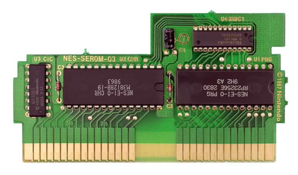
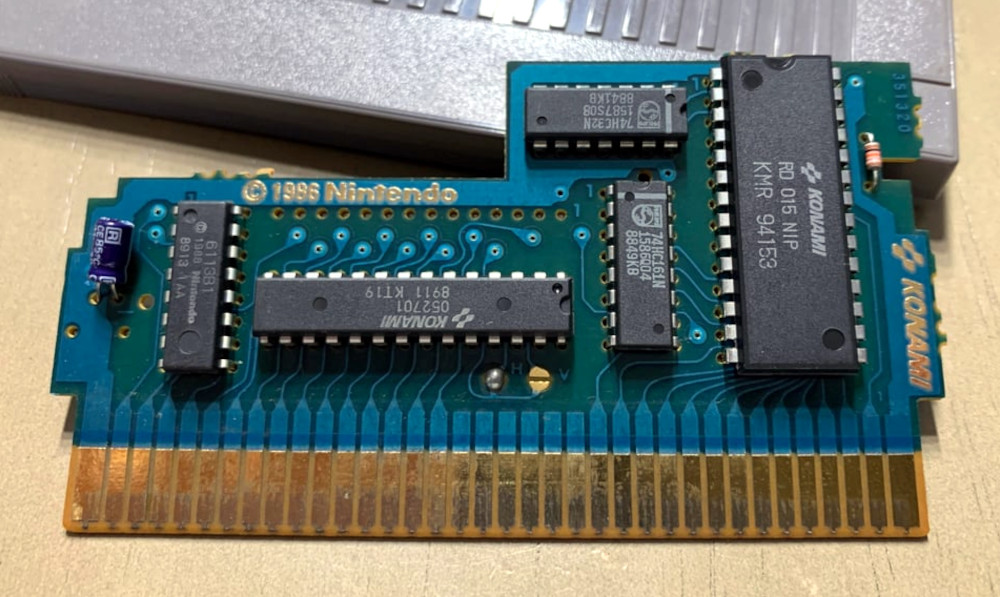
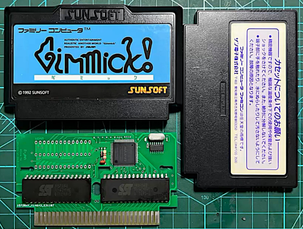
The shell protects a small PCB. Depending on the game, it may include:
- PRG-ROM: the program, but also levels, text, music sequences, or compressed data;
- CHR-ROM: graphic patterns directly accessible to the PPU;
- CHR-RAM, generally instead of CHR-ROM: a graphic memory the program fills and can modify;
- Additional RAM, used as working memory or for save data;
- logic for bank selection, synchronization, and sometimes audio generation.
PRG and CHR mainly describe the role and connections of those memories. PRG-ROM thus doesn’t only contain instructions. Some boards even combine CHR-ROM and CHR-RAM.
In a typical battery-backed save cartridge, a battery keeps a RAM powered when the console is off. The saved part is not written into game ROM. Other save technologies exist; see the media evolution section.
The game is usually not fully loaded into the console
With a typical cartridge, the CPU usually reads its instructions directly from the cartridge ROM via the connector and buses. The PPU can, in turn, read patterns from CHR-ROM.
There is thus no need to copy the entire game into the 2 KiB of RAM before running it. That doesn’t prohibit copying, preparing, or decompressing some data while running.
The apparent limit: 32 KiB of program and 8 KiB of patterns
A simple NROM cartridge typically has 16 or 32 KiB of PRG-ROM and 8 KiB of CHR-ROM. With only 16 KiB of program, the same ROM appears twice in the CPU’s 32 KiB window.
Yet many games go far beyond those sizes. They use a mapper: the cartridge logic that organizes the memory visible to the console.
Bank switching: changing which page is visible
Bank switching splits memory into blocks and chooses which ones appear at certain addresses.
Imagine a 64 KiB ROM divided into four 16 KiB banks, named A, B, C, and D. A common setup changes the bank visible in the lower half of the window while keeping the last bank fixed in the upper half:
| State | $8000–$BFFF |
$C000–$FFFF |
|---|---|---|
| Before command | Bank A | Bank D, fixed |
| After selecting B | Bank B | Bank D, still fixed |
We don’t copy 16 KiB to make this change. The circuit modifies the logical connections between addresses and memory. It’s like looking at a different page through the same window.
The CPU keeps sixteen-bit addresses, but can successively access a much larger amount of memory. The same principle applies to the pattern memory the PPU sees.
A write to an area normally read as ROM may instead command the mapper: it does not necessarily modify the ROM itself.
Not all mappers are big specialized chips
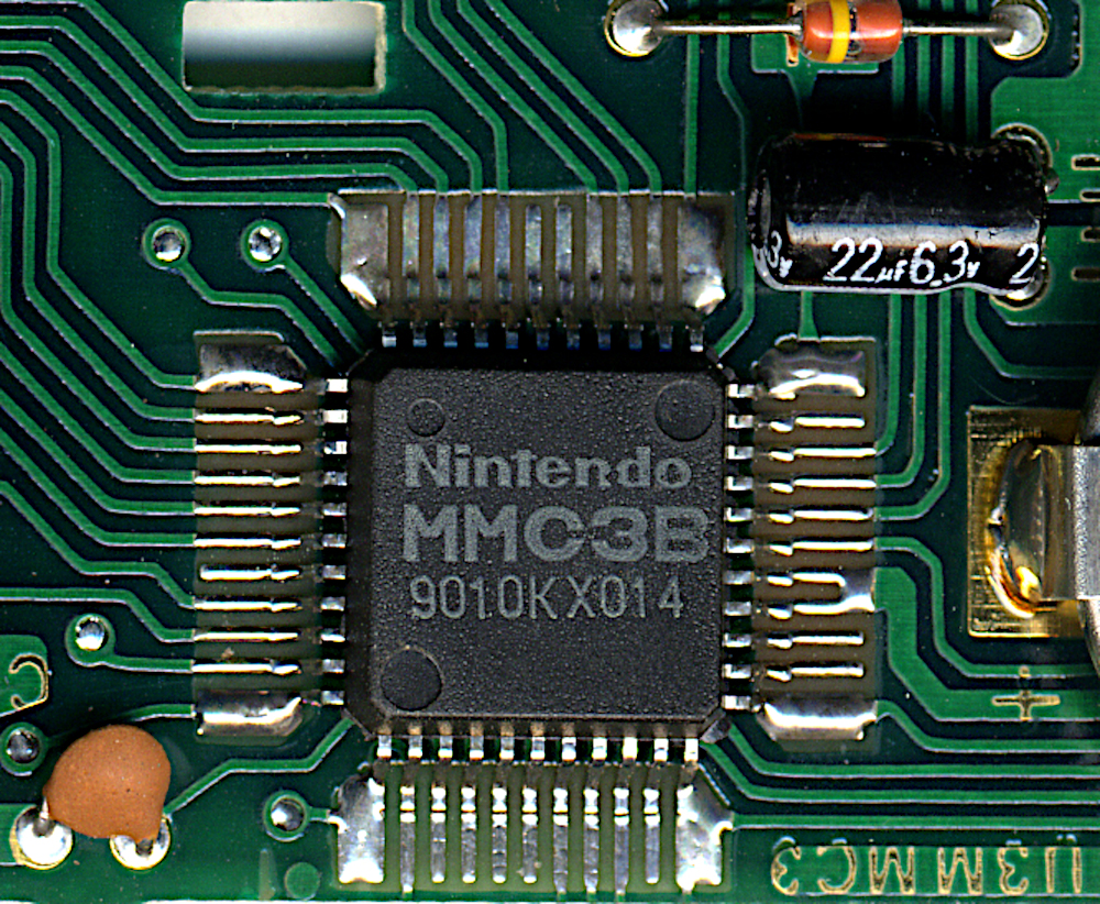
Some boards use a few simple logic components. Others integrate a specialized chip, like MMC1 or MMC3 from Nintendo. Even the fixed NROM organization is called “mapper 0” in emulation formats, though it performs no active switching.
Depending on the model, the mapper can also manage RAM, organize background maps, produce interrupts useful for visual effects, or add sound. This hardware explains part of the dramatic evolution of games without changing consoles.
For more: board families and mappers.
5- How the console builds an image
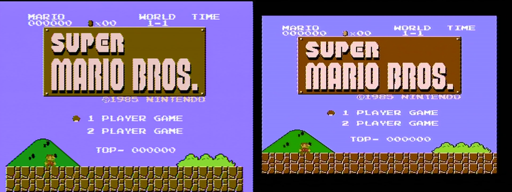
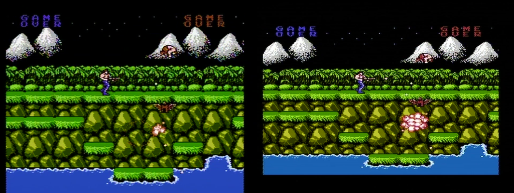
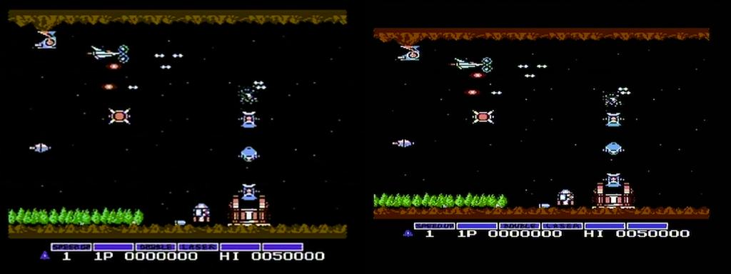
The PPU is generally a Ricoh 2C02 on NTSC machines, or a 2C07 on PAL NES units. The logical image is 256 × 240 pixels. Timing differences are detailed in the regional section.
Not one big complete image to redraw in memory
The NES does not primarily rely on a framebuffer, i.e., a memory holding the color of each pixel in the full image. Instead, the PPU assembles the image during scanout, line by line, from reusable elements.
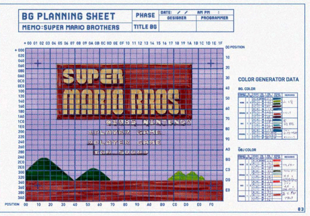
It’s like a mosaic: you keep a collection of patterns, then a map indicating where to place them. The CPU doesn’t have to recompute every pixel of a wall made of identical bricks.
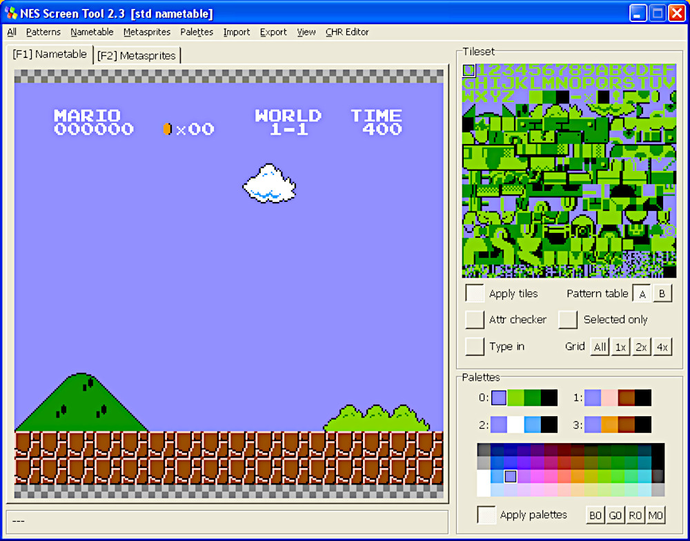
Tiles: 8 × 8 pixel patterns
A tile measures 8 × 8 pixels. Each pixel is described by two bits, which select one of four values. These values are color indices, not directly red, green, and blue components.
8 × 8 pixels × 2 bits = 128 bits = 16 bytes per pattern.
The data is organized in two bitplanes: one plane provides the first bit of each pixel, and the second plane provides the other bit.
The 8 KiB of patterns visible at a given time can contain 512 patterns of 8 × 8 pixels, split into two tables of 256 patterns. Which table is used depends on PPU settings and on the element type.
The background: a tile map and attributes
A nametable describes a grid of 32 × 30 tiles, i.e., a 256 × 240 pixel screen. Each entry essentially says: “at this position, use this pattern.”
That’s 960 tile indices. A table of 64 attribute bytes complements this by choosing palettes, normally per 16 × 16 pixel regions. The whole set is exactly 1 KiB.
Multiple positions can reuse the same pattern. So a row of twenty bricks does not require twenty distinct brick drawings in memory.
Sprites: elements placed independently of the background
A sprite is a small graphic element positioned independently of the background. It can represent part of a character, a projectile, an item, or an effect.
- The primary OAM holds 64 sprite entries.
- Sprite size is 8 × 8 or 8 × 16 pixels, depending on a global PPU setting.
- The PPU retains at most eight sprites per line in standard operation.
Each entry uses four bytes: position, pattern index, and attributes such as palette, horizontal or vertical flip, and priority relative to the background. A large character is typically composed of multiple sprites.
If too many sprites are on one line, some won’t be displayed. Many games change sprite ordering from one frame to the next to spread out the disappearances: this creates the characteristic flicker. This alternating flicker is often a deliberate programming strategy, not an automatic fixed effect of the PPU.
Palettes and colors
The PPU uses 64 base color codes. They don’t correspond to 64 all-distinct colors: several codes can produce identical or very similar results. Exact rendering also depends on the analog signal, the TV, and, in emulation, the chosen conversion palette.
A palette is a small list of colors. The values in patterns select an entry from that list. In the common case:
- the background has four palettes of three colors, plus a shared background color: 13 colors;
- sprites have four palettes of three colors, with their fourth value being transparent: 12 additional colors.
That yields up to 25 simultaneously selected colors in a standard image. This isn’t an absolute limit on all effects: changing palettes or certain settings during scanout can produce other results.
Scrolling and background maps
Scrolling moves the window over the background. During movement, the program refreshes portions that are about to enter the screen.
The PPU provides addresses for four background maps, but the console typically has enough RAM to store two. The cartridge determines how the four logical slots map to those two physical memories: this is called nametable mirroring. Some boards add RAM to have four distinct maps.
Names can be misleading: vertical mirroring repeats maps top-to-bottom and usually leaves two distinct maps side by side, so it’s often used for horizontal scrolling. Horizontal mirroring does the opposite. These names describe memory repetition, not a mandatory scrolling direction.
From logical image to the TV
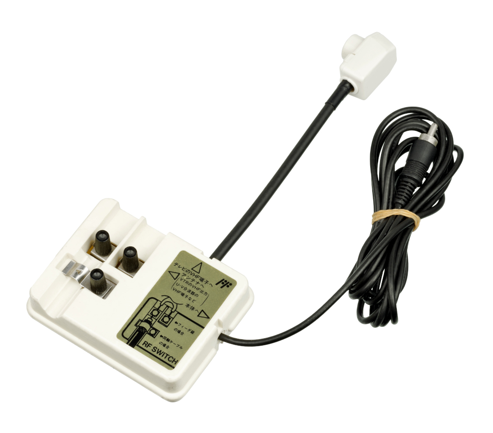
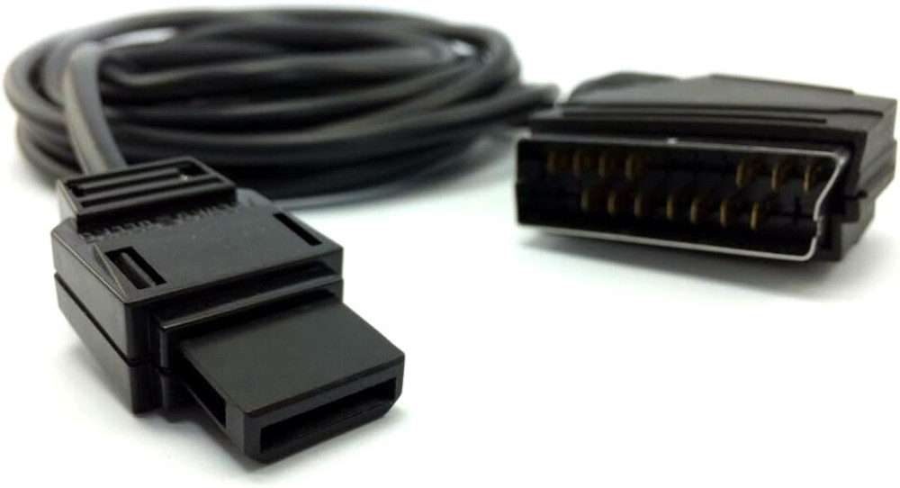
The result is sent as an analog video signal. Original models commonly use composite video or an RF output intended for the antenna input. In France, the SCART connector was commonly used.
The signal is low-definition and non-interlaced in typical use, often described as “240p” for NTSC machines. Logical pixels need not be considered square on a TV. In addition, overscan can mask part of the image edges.
For more: PPU memory, rendering, and palettes.
6 – How the console reads controllers and produces sound
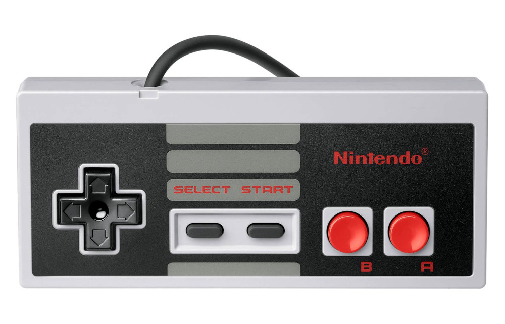
A standard controller transmits eight states
The eight inputs are: A, B, Select, Start, Up, Down, Left, and Right. These are digital inputs: each button is pressed or released. The D-pad does not indicate an analog angle.
A shift register
captures the state of the buttons, then presents it
one bit at a time.
The program commands this capture by writing to
$4016, then reads the successive states:
- via
$4016for the first controller; - via
$4017for the second.
“Button A is pressed” does not inherently mean “jump”: the game program assigns that meaning.
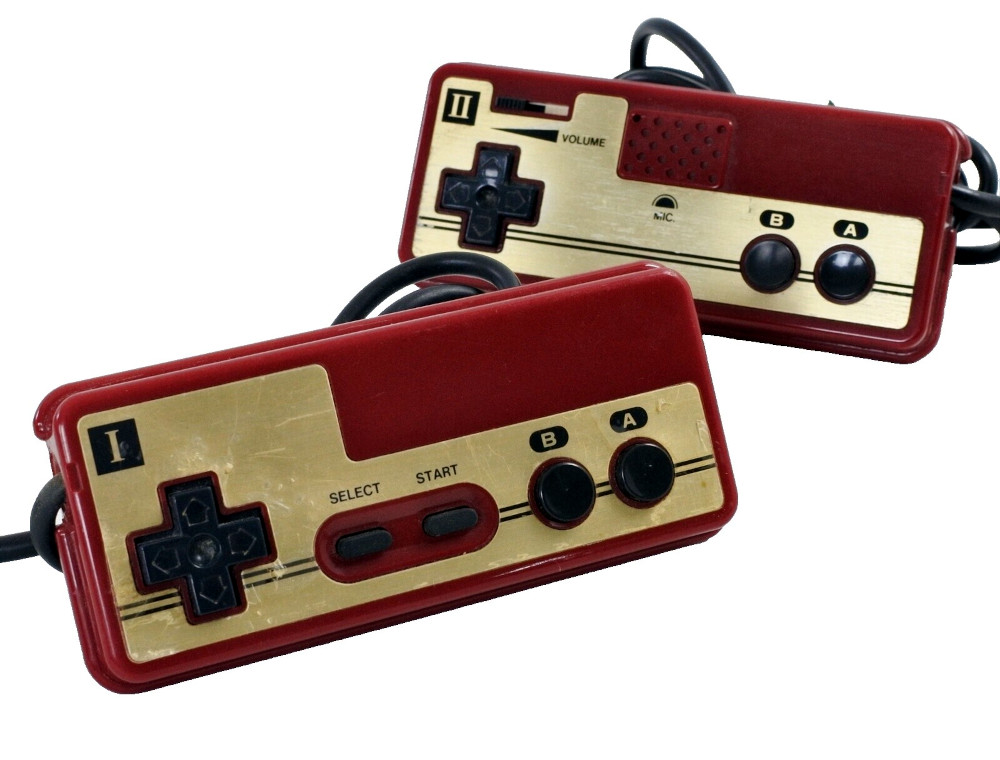
The original Famicom has a peculiarity: its second controller lacks Start and Select, but includes a microphone. It provides a rudimentary sound detection; it’s not an input for recording a voice like on a modern computer.
The APU has five basic sound channels
A sound channel is a generator that the program can configure. Several channels run simultaneously and are mixed. The APU integrated into the main chip provides:
- Two pulse (rectangular) channels, often used for melodies and harmony parts.
- One triangle channel, often used for bass lines.
- One pseudo-random noise channel, useful for percussion and many sound effects.
- One DMC channel, which reads audio data coded as successive level changes.
For DMC, each bit usually commands a small increase or decrease of an accumulated level. This delta coding is neither MP3 nor simply a stream of eight-bit amplitude samples.
Music is usually stored as notes, durations, and parameters, possibly with samples. A game routine translates that data into APU settings. The APU then continues producing audio while the CPU handles other tasks.
Additional audio can come from the cartridge
The Famicom routes audio through the cartridge connector. An extra circuit can thus add its sounds to those of the console. The Disk System and some cartridges using chips like VRC6, VRC7, or Sunsoft 5B leverage this.
The NES 72-pin connector does not carry this audio path in the same way. A simple cartridge adapter therefore does not guarantee reproduction of a Famicom game’s extra audio. Official NES versions are generally designed around the five internal channels.
“8-bit console” does not mean “8-bit sound.” CPU data width, a sample’s encoding, and how a circuit produces a waveform are distinct characteristics.
For more: controller reading and APU and audio expansions.
7- From startup to the game loop
How does the program start?
The CPU has a hardware startup mechanism.
Upon reset, it reads two bytes at addresses
$FFFC–$FFFD.
Together they form a sixteen-bit address:
the RESET vector, which indicates
where to begin execution.
With a typical cartridge, these bytes come from the cartridge memory. The program then initializes the data it needs and configures the circuits. Initial RAM content must not be assumed reliable.
The cartridge-based console does not have an operating system that launches all games. On models equipped with it, the CIC lockout (Checking Integrated Circuit, often called the 10NES system) must still allow a stable startup. The Disk System is another case: it brings its own BIOS.
Example: making a character jump
- Read inputs. The game detects that the player has just pressed A.
- Update game state. It gives the character a vertical speed, updates position, then tests collisions.
- Prepare display changes. It builds new sprite descriptions in RAM and a list of background updates.
- Transfer data at the right moment. It typically uses the interval between visible frames to update video memories.
- Display the new state. The PPU builds the next image from available information.
Collisions are usually computed from positions and level data, not by analyzing the colors shown on the TV.
VBlank: a window for updates
Between visible frames is the VBlank, or vertical blanking interval. It’s a particularly suitable time for transfers to the PPU, because the PPU is no longer reading those same memories to draw the visible scene.
At the start of VBlank, the PPU can trigger a NMI, if the program has enabled it. This interrupt temporarily makes the CPU run a specific routine before resuming prior work.
A DMA notably allows transferring the 256 bytes of sprite descriptions to OAM without a copy loop of instruction-by-instruction loads/stores. The CPU is however halted during this transfer: DMA doesn’t make the operation free.
Available time is limited. Games therefore spread some updates over multiple frames or leverage carefully synchronized changes during scanout. The exact organization varies by program.
Why can a game slow down?
If computations are not finished in time, a game may keep the same state for several frames. The video cadence may remain stable while the game itself advances more slowly. It’s not necessarily the CPU clock that slows down.
This phenomenon differs from sprite dropouts caused by the eight-sprites-per-line limit.
8- Regional differences: more than another shell
Main hardware versions
The words NTSC and PAL designate families of analog TV standards. For the NES, they are also used to distinguish hardware variants whose clocks and frame rates are not identical.
| Characteristic | Japanese Famicom | NTSC NES | PAL NES |
|---|---|---|---|
| Representative markets | Japan | North America | Much of Europe, Australia |
| CPU/APU chip | Ricoh 2A03 | Ricoh 2A03 | Ricoh 2A07 |
| Typical PPU | Ricoh 2C02 | Ricoh 2C02 | Ricoh 2C07 |
| CPU frequency | ≈ 1.7898 MHz | ≈ 1.7898 MHz | ≈ 1.6626 MHz |
| Frames per second | ≈ 60.10 | ≈ 60.10 | ≈ 50.01 |
| Scanlines per frame | 262 | 262 | 312 |
| Game’s logical image | 256 × 240 pixels | 256 × 240 pixels | 256 × 240 pixels |
| Cartridge connector | 60 pins | 72 pins | 72 pins |
| CIC on classic models | No | Yes on front-loading NES | Yes on front-loading NES |
The additional PAL scanlines don’t automatically become extra graphics lines usable by the game. The division between active image, borders, and blanking intervals differs, as do the proportions on a TV set.
Why are some PAL games slower?
Suppose a game moves an object by one pixel per frame. At about 60 frames per second, it advances ~60 pixels per second. If the same principle is kept at 50 frames per second, it advances only 50 pixels per second.
A port that fails to compensate for this difference may therefore be about 17% slower. But this is not universal: some PAL games were adjusted, wholly or partially.
Distinguish this frame cadence difference from that of the CPU: the PAL CPU is only about 7% less clocked than the NTSC CPU. Frame duration, available transfer time, and the CPU/PPU clock relationship also change.
Audio needs adjustments too: produced frequencies for some settings and channel timings differ. A port may thus have to correct tempo, note pitches, and effect synchronization.
Connectors, controllers, and video outputs
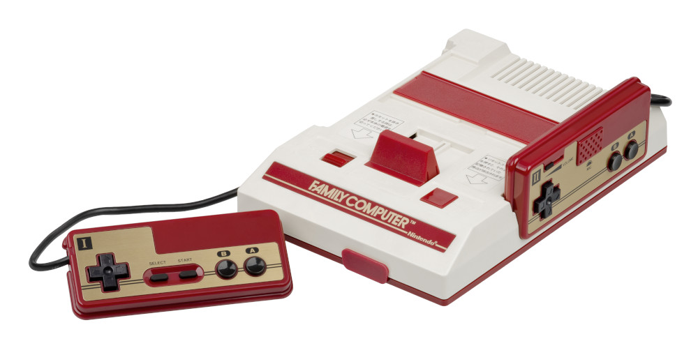
- Original Famicom: 60-pin cartridges, two controllers attached to the console, a microphone on controller 2, a front expansion port, and RF output for the Japanese market.
- Classic NES: 72-pin cartridges and detachable controllers. Video outputs vary by country and model; many front-loading NES units offer RF and composite.
- 1993 AV Famicom: detachable controllers and composite output, without the controller-2 microphone of the original.
- Top-loading NES: the North American NES-101 typically lacks the CIC and usually provides RF output.
Some French NES units provide RGB via SCART after converting an internal composite signal. An RGB connector thus does not necessarily mean that the PPU natively produces an RGB image.
The twelve extra pins of the NES cartridge do not make the processor “wider.” Signal assignments differ, notably for lockout and expansions; the Famicom’s audio lines are not simply preserved.
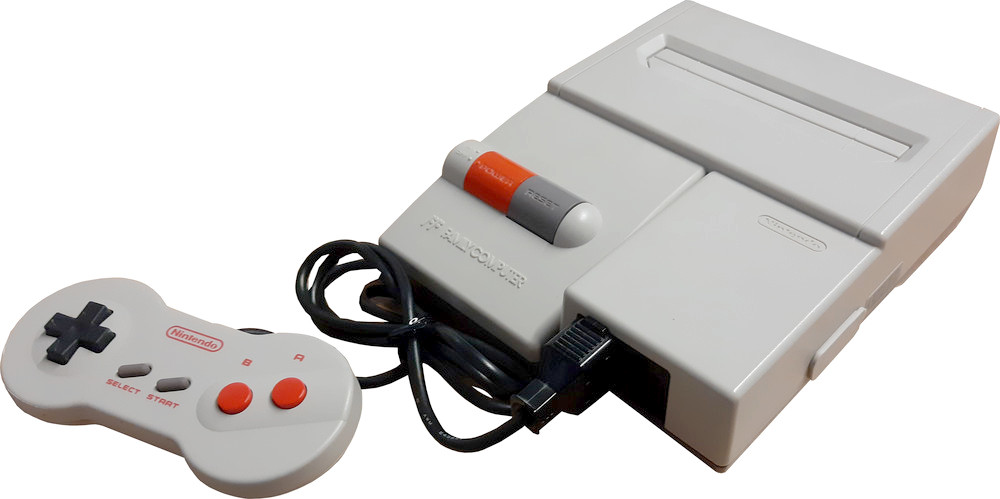
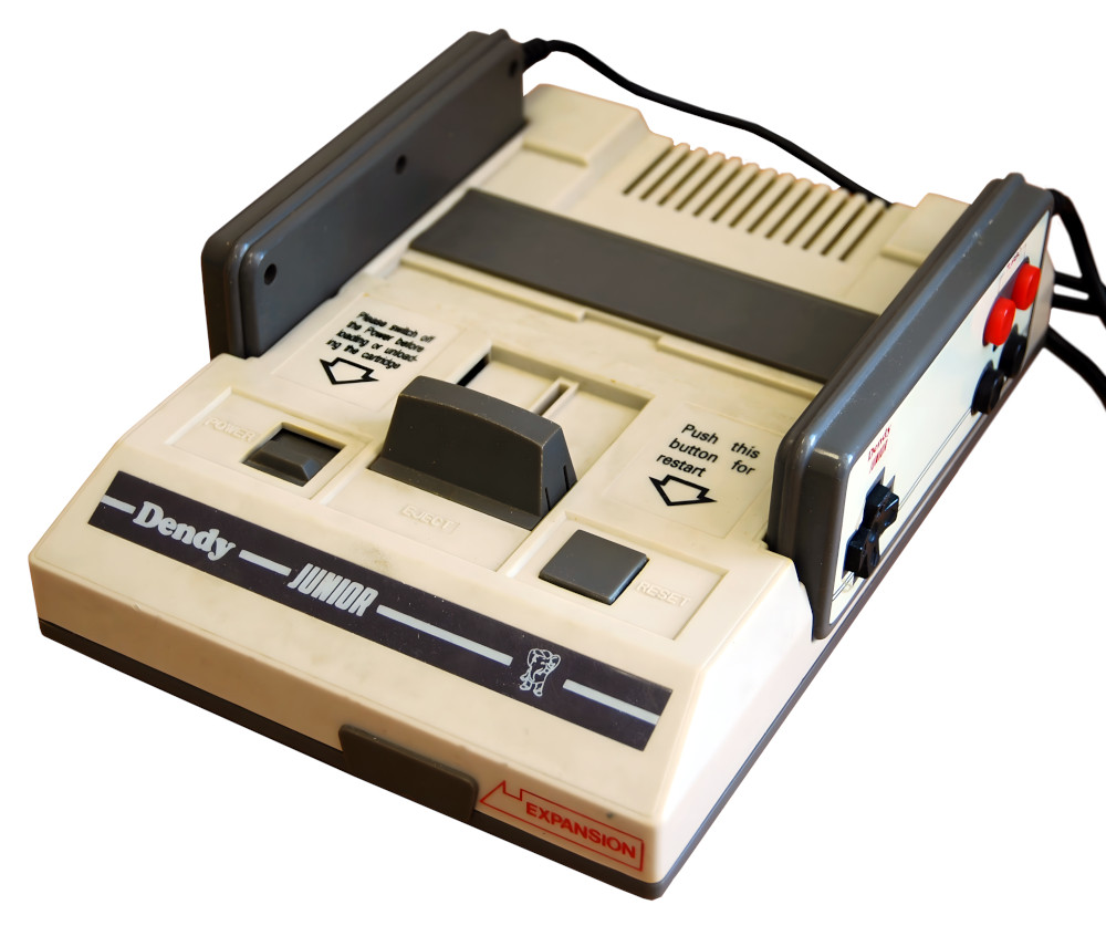
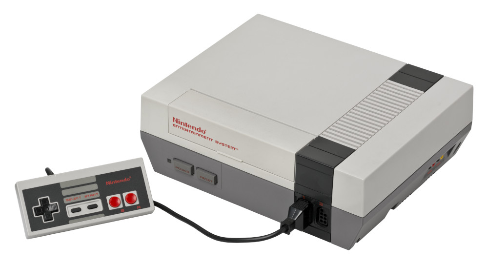
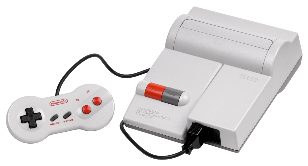
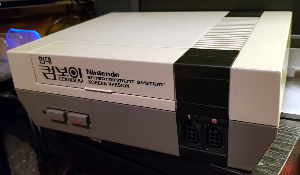
Beware of clones and commercial names
Not all compatible devices exactly follow Nintendo’s variants. Clones often called Dendy, for example, combine a 50 Hz video cadence with synchronization choices differing from those of an official PAL NES. A “50 Hz” label is thus not enough to identify the architecture.
Inserting a foreign game does not change the console’s clock. A cartridge adapter does not turn a PAL NES into an NTSC NES, nor is it by itself a video signal converter.
For more: clocks and NTSC/PAL differences.
9- The 10NES/CIC lockout and regional compatibility
Two circuits that must communicate
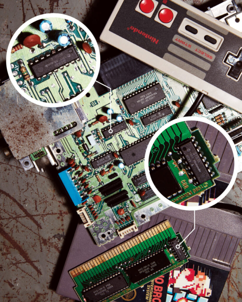
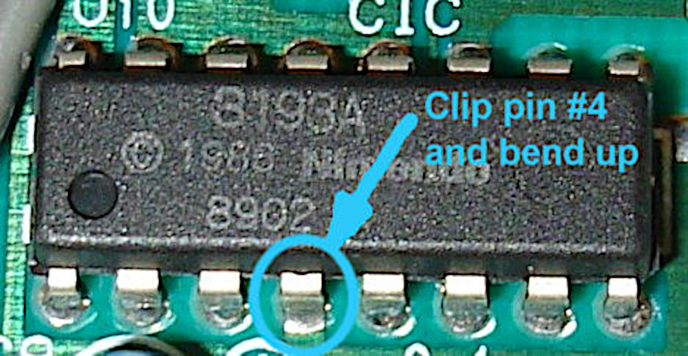
On front-loading NES units, the 10NES/CIC system uses two chips: one in the console, playing the role of the “lock,” and one in the cartridge, playing the role of the “key.”
The two chips must carry out a compatible exchange and stay synchronized. If the exchange is missing or not as expected, the console’s chip triggers resets that prevent stable operation.
This system is used to control authorized cartridges and to separate certain markets. It does not read the entire program to verify authentic content and it does not decrypt game graphics.
Regional groups aren’t limited to NTSC vs PAL
NTSC NES units and different PAL NES groups do not all use compatible keys. In common labels:
- PAL-A covers the UK, Italy, Australia, among others;
- PAL-B covers most of the other European markets, notably France and Germany.
In this context, PAL-A and PAL-B designate NES compatibility groups. They should not be confused with similar labels for broadcast TV systems. Both PAL NES groups remain machines at about 50 frames per second.
The Famicom does not have this lockout
The Japanese Famicom does not have a CIC, and its ordinary cartridges do not include the corresponding key. The top-loading North American NES-101 also lacks it. The absence of a CIC does not, however, remove differences in the connector or synchronization issues.
Three distinct questions for an imported game
| Question | Possible obstacle |
|---|---|
| Can you connect the cartridge? | Shell shape, 60-pin or 72-pin connector, and signal mapping. |
| Will the console allow a stable startup? | Presence of a compatible CIC key if the console uses this lockout. |
| Does the program run correctly? | NTSC/PAL cadence, synchronized effects, extra audio, accessories, and signal accepted by the TV. |
Some adapters have a compatible key or use one from another cartridge. A console may also be modified to disable its lockout. These solutions do not automatically correct frequency or audio-path differences.
Why can the NES LED blink?
A poor contact can prevent CIC communication. On a front-loading NES, this can cause the famous blinking LED and repeated resets. A cartridge from the correct region can thus show this symptom.
Conversely, not all image or startup issues are due to the CIC: the contacts also carry the addresses, data, and signals needed for the game to function.
For more: CIC operation and variants.
10- The Famicom Disk System: games on disks
A Japanese accessory launched in 1986
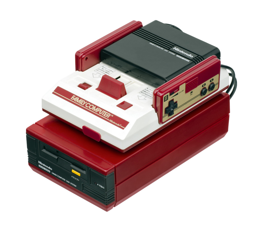
The Famicom Disk System, or FDS, lets the Famicom use Disk Cards: small proprietary magnetic disks derived from Mitsumi’s Quick Disk technology. These are neither optical discs nor 3.5-inch PC floppies.
The goal was to offer a rewritable, economical medium at a time when large ROMs were expensive. A single disk could hold a game and, if designed for it, save data.
The FDS was officially marketed for the Japanese market, not as a standard extension for Western NES units. The Sharp Twin Famicom combines a Famicom and a Disk System-compatible drive in one device.
Two parts: the drive and the RAM Adapter
The drive does not plug directly in place of a cartridge. It is connected to a RAM Adapter, which is inserted into the Famicom’s cartridge port.
This adapter provides memory, a BIOS, and a control chip including disk functions and audio. The main CPU and PPU remain those of the console.
| Memory | Address or access | Role |
|---|---|---|
| 32 KiB RAM | CPU: $6000–$DFFF |
Program and data loaded from disk. |
| 8 KiB BIOS ROM | CPU: $E000–$FFFF |
Startup, loading functions, and hardware services. |
| 8 KiB CHR-RAM | PPU: $0000–$1FFF |
Graphic patterns loaded or constructed by the program. |
This time, the program must be loaded into RAM
A cartridge ROM responds directly to reads on the bus. A disk must physically spin under a read head. The CPU cannot execute instructions directly from the magnetic surface.
Operation therefore follows this principle:
- the BIOS starts from the RAM Adapter’s ROM;
- the drive provides the data of the inserted side;
- routines transfer the required files into RAM;
- the CPU executes the program now present in this RAM;
- the game reloads other data when necessary.
Data on a side is traversed essentially in sequence. The drive does not freely seek to tracks and sectors like a classic PC floppy drive. This explains the loading delays.
Capacity, sides A and B, and disk swaps
A commonly cited order of magnitude is about 64 KiB per side. The space actually available for files depends on block organization and spacing. Distinguish this capacity from the conventional size of disk image files.
A game may use one side, both sides of a card, or multiple cards. The drive uses one side at a time: the player must physically flip the disk when the game requests it.
A large amount of data on disk does not become that much more RAM. The program must organize what remains in memory and what must be reloaded.
Saving to disk
When the game supports it, the drive writes data back to the magnetic surface. It persists without a battery. The game must explicitly handle this save; simply using a disk does not guarantee that all progress is preserved.
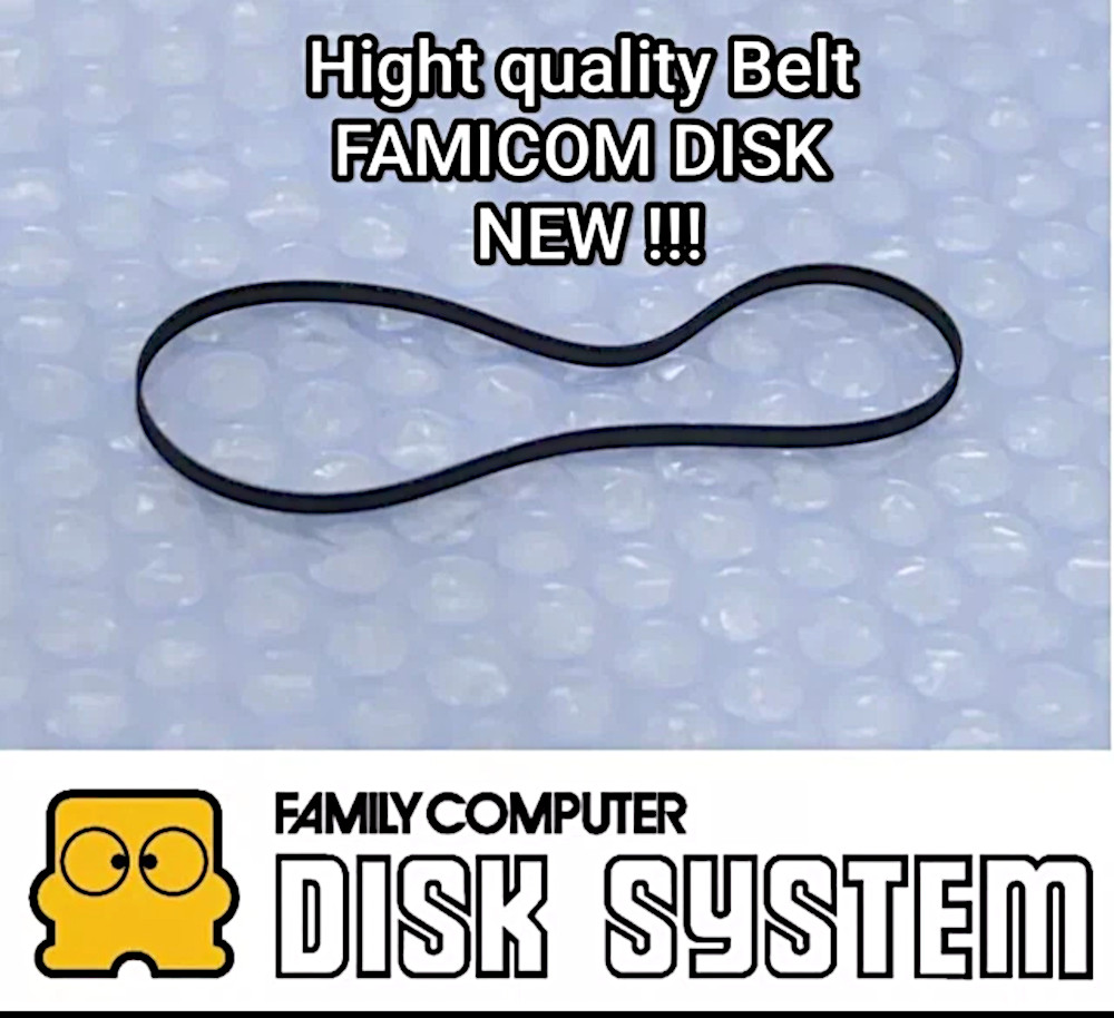
In return, the medium and the drive are mechanical: wear, surface condition, head alignment, and belt aging can affect reads or writes. Do not interrupt an ongoing write.
An additional sound channel
The FDS adds a programmable wavetable channel with a modulation mechanism. The program can define the shape of a small repeated waveform, which yields timbres beyond the ordinary internal generators.
This expansion explains some musical differences between an FDS version and its NES cartridge adaptation. The FDS does not replace the APU: it adds a sound source.
Protections different from CIC
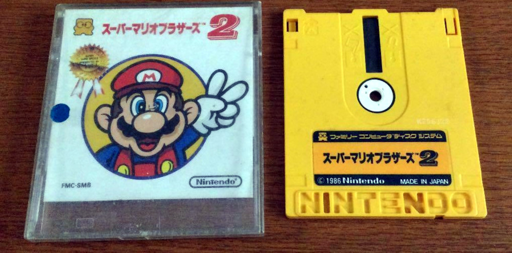
The FDS relies on a Famicom without CIC. It therefore does not use the NES cartridge key-based lockout. It uses other constraints: mechanical peculiarities of the shell, including the molded “Nintendo” marking, and format or identification checks performed by the BIOS. Some games add their own verifications.
These mechanisms should not be confused with PAL-A/PAL-B zoning. The official FDS belongs to the Japanese NTSC ecosystem. Adapting it to a foreign NES raises connector, synchronization, and audio questions.
For more: FDS architecture, BIOS, and disk format.
11- Media types and their technological evolution
Exterior shape doesn’t reveal all the electronics
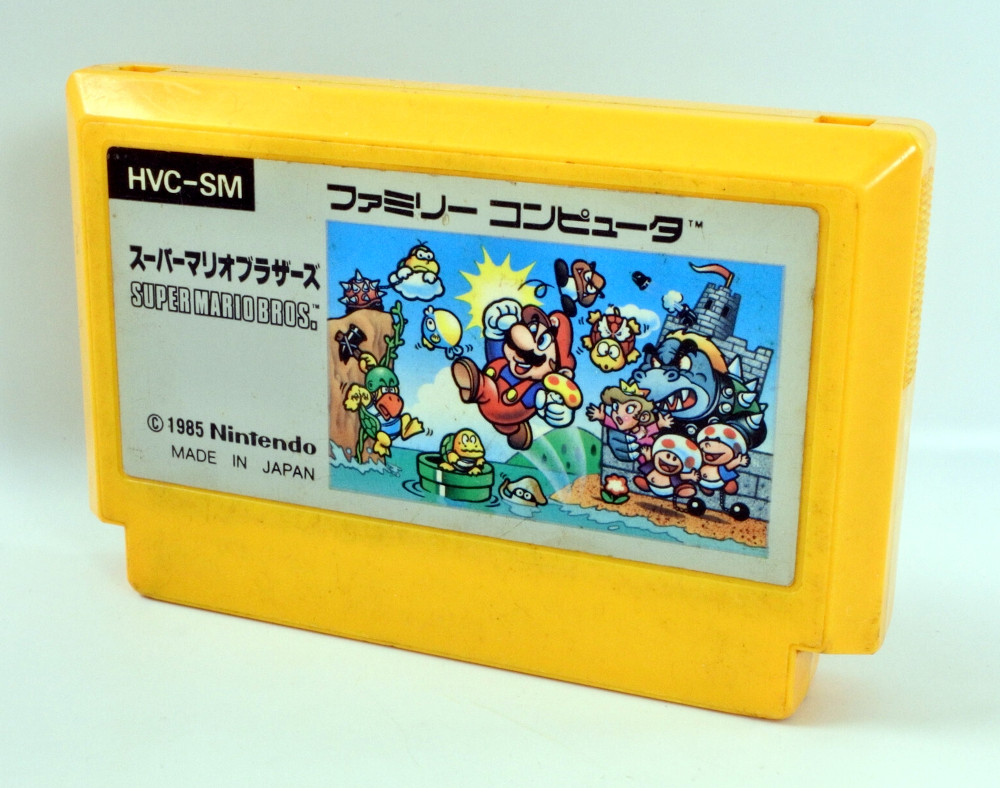
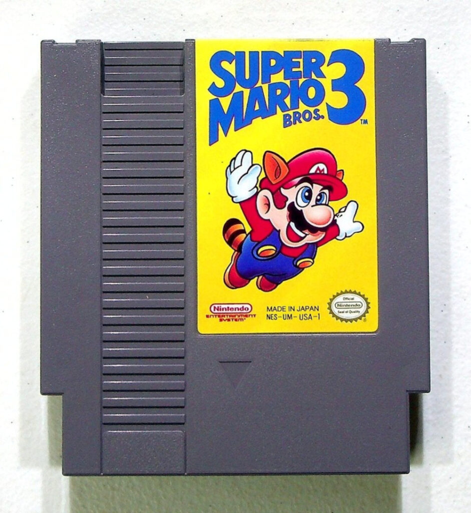
Famicom cartridges come in various shapes and colors, typically with 60 pins. Official NES cartridges generally use a larger 72-pin shell. The plastic’s color and size don’t indicate memory size or mapper functions.
Two cartridges that look identical on the outside may carry very different circuitry. To compare them technically, you must examine their PCB, memories, and control logic.
From simple boards to specialized chips
| Family or period | Technical principle | What it brings |
|---|---|---|
| Fixed cartridges, notably NROM | Program and graphics directly wired, no active bank switching. | Low cost and immediate access. Super Mario Bros. uses, for instance, 32 KiB PRG-ROM and 8 KiB CHR-ROM. |
| Simple logic: CNROM, UxROM, AxROM… | A few components select banks. CNROM mainly switches CHR-ROM; UxROM switches PRG-ROM and generally uses CHR-RAM. | More graphics or more program, without complex chips. Exact possibilities depend on the board. |
| FDS, from 1986 | Rewritable magnetic medium, data loaded into the RAM Adapter. | Economical distribution, disk saving, in-store rewriting, and extra audio, but with loading waits and mechanics. |
| MMC1, late 1980s | More flexible PRG/CHR banking and background organization; RAM depending on the board. | Larger games and possible battery saves. The NES version of The Legend of Zelda is an example. |
| MMC3, late 1980s and beyond | Finer banks and an interrupt counter tied to PPU activity. | Flexible graphics management and synchronized effects, e.g., to separate a game area from a fixed status bar. Super Mario Bros. 3 uses this family. |
| Specialized chips: MMC5, VRC, Sunsoft… | Functions unique to each chip: advanced memory management, graphics extensions, or additional sound channels. | MMC5 can extend background attributes, for example; VRC6, VRC7, and Sunsoft 5B add sound on Famicom. |
| Modern rewritable carts | Flash memory, RAM, and programmable logic, sometimes with a removable memory card. | Development, homebrew, and support for multiple cartridge organizations, depending on the hardware’s capabilities. |
This list isn’t exhaustive. Other families, like MMC2 and MMC4, use bank changes linked to patterns read by the PPU. MMC numbers do not form a simple ladder where each model is superior in all areas.
Likewise, the MMC3’s counter is not a universal clock that “understands” the image: it observes certain PPU signals. The program must use it with the circuit’s real behavior in mind.
CHR-ROM or CHR-RAM: two choices, not simply two generations
With CHR-ROM, patterns are already present. A mapper can quickly select different banks. With CHR-RAM, the program can generate, decompress, or load new patterns, but must transfer their data at the right time.
CHR-RAM is not automatically more modern or superior. It offers different flexibility with different constraints.
Factory ROMs, prototypes, and rewritable memories
- Factory ROM with fixed content: common in mass-market releases; the content is set at manufacturing time.
- EPROM: programmable memory, used notably for prototypes and development; some versions are UV-erasable.
- EEPROM and Flash: electrically erasable and non-volatile. Some historical carts use an EEPROM to save; modern carts may use Flash to store games.
Programmable logic in a modern cart, sometimes an FPGA, can reproduce several mappers. But a large memory card does not guarantee universal compatibility: graphics, audio, and each mapper’s peculiarities must also be reproduced.
Unlicensed cartridges and multi-game compilations form further variants. A compilation may use special selection logic; its number of games doesn’t itself indicate the amount of distinct content.
Disk Cards and associated services
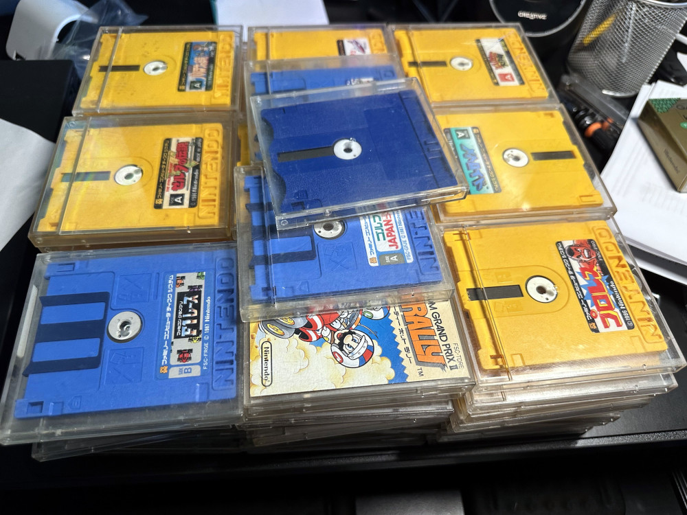
- Ordinary Disk Cards, often yellow: the game may use one or both sides. These media generally lack the protective shutter of a modern PC floppy.
- Disks rewritten with the Disk Writer service: kiosks in Japanese stores allowed replacing the content with another game in the catalog. This is a distribution method, not a new disk capacity.
- Disks tied to the Disk Fax service, often blue: certain contest games allowed saving results, then transmitting them from an in-store kiosk. The home FDS did not thereby become a console equipped with a modem.
- Games on multiple sides or multiple cards: they increase the total amount of data available, but not the RAM in the RAM Adapter.
A side A and side B are simply the two sides of a disk: these letters are unrelated to the PAL-A and PAL-B NES cartridge groups.
Why did cartridges regain the upper hand?
As ROM prices fell, cartridges could offer much more content without mechanics or comparable read waits to those of a disk. Mappers grew in flexibility and save memories brought a function that had been an important advantage of the FDS.
Cartridge games thus reached several hundred KiB, or more depending on the chips used. The Disk System’s decline does not correspond to disks transforming into a new, larger-capacity format: mostly, cartridge economics and electronics evolved.
For more: mapper documentation and history of media and FDS services.
12- What really changes with a “16-bit” console
Now that CPU, buses, and graphics hardware roles are separated, the expression “16-bit console” is clearer. It summarizes an architecture and a commercial generation, not an identical property of all components.
Twice the bits, but 256 times the combinations
- A 8-bit chunk offers 256 combinations, i.e., unsigned integers from 0 to 255.
- A 16-bit chunk offers 65,536 combinations, i.e., unsigned integers from 0 to 65,535.
Adding eight bits multiplies combinations by 256. It does not multiply compute speed by 256, nor even automatically by two.
A processor with sixteen-bit operations can more directly manipulate certain values: e.g., a position of 3,000 pixels in a level. An 8-bit CPU can achieve the same result by using multiple bytes, often with more instructions.
What the bit width alone does not tell you
- Actual speed: it depends on frequencies, instructions and their cycles, memory access, and program organization.
- Amount of RAM: data width does not dictate address width nor how many memory chips are installed.
- Graphics capabilities: colors, sprites, and effects depend mainly on video hardware. The SNES’s Mode 7 comes from its graphics hardware, not automatically from its 16-bit CPU.
- Sound or image formats: “16-bit audio” and “16-bit per pixel image” describe data formats, not the CPU category.
A sixteen-bit value takes two bytes, but a 16-bit CPU does not force all data to be stored as sixteen-bit values. It can also process many operations on bytes.
For more: architectures of the SNES and Mega Drive.
Example: NES and Super Nintendo
| Characteristic | NES / Famicom | Super Nintendo |
|---|---|---|
| Main chip | Ricoh 2A03 or 2A07, 6502-derived core | Ricoh 5A22, 65C816-derived core |
| Common integer operations | Mainly 8-bit | 8 or 16-bit depending on settings |
| External CPU data bus | 8-bit | 8-bit |
| Address width | 16-bit | 24-bit |
| CPU address space | 64 KiB | 16 MiB |
| Main work RAM | 2 KiB | 128 KiB |
The SNES nicely illustrates the distinction between computation and data transport: its CPU can perform a sixteen-bit operation while receiving the two bytes successively over an external eight-bit bus.
Picture a table wide enough to handle two objects together, but a door that only lets one object pass at a time. Table width and door width are two independent characteristics.
And the Mega Drive?
Its main CPU, the Motorola 68000, has 32-bit data registers and a 16-bit external data bus. It’s often described as a 16/32-bit processor, while the console is commercially associated with the “16-bit” generation.
13- Game files and emulation
A .nes file describes a cartridge, not just a program
A .nes file typically contains an
image of the ROM memories from a cartridge,
preceded by a header in iNES
or NES 2.0 format.
This header indicates notably memory sizes and the mapper to reproduce. NES 2.0 allows more precise descriptions of hardware variants, memory, and sync conditions.
This header is a file convention. It’s not a universal header that the CPU reads in all physical cartridges. It does not replace a CIC key.
A .fds file represents disk sides
The common .fds format reserves
65,500 bytes per side, with an optional
sixteen-byte file header.
Do not confuse this conventional size with the amount
of useful data for a given game.
The file represents blocks and their contents, but typically does not preserve all details of the magnetic signal, spacing, and checks present on the physical medium. Other preservation formats may retain different information or something closer to a raw read.
The RAM Adapter’s 8 KiB BIOS is normally not included in the disk image. FDS emulation thus generally requires a copy of this BIOS or a compatible replacement.
What an emulator does
An emulator reproduces in software the behavior of the CPU, PPU, APU, memories, and the media-specific circuits. The game file is not directly a PC program.
In particular, a mapper is originally hardware, not just code hidden in ROM. To reproduce a game correctly, it may be necessary to respect its banks, interrupts, and synchronization peculiarities.
Emulation must also select the correct NTSC, PAL, or other characteristics. Changing this setting does not automatically transform one program version into a properly adapted port for another region.
Finally, an emulator save state differs from a game-provided save: it captures a snapshot of the emulated machine’s state rather than only reproducing the data written to a cartridge RAM or a disk.
For more: iNES, NES 2.0, and FDS formats and emulation and debugging tools.
14- Key takeaways
- The CPU runs the game’s rules; the PPU and APU build image and sound. They operate in parallel.
- 8-bit, 16-bit addresses, and MHz describe different things. Data width alone does not fix RAM, number of colors, or speed.
- The PPU assembles tiles and sprites. It does not primarily rely on a full image stored pixel by pixel.
- The cartridge is part of the architecture. Its memories and mappers enable more ambitious games to run on the same console.
- Connector, regional lockout, and synchronization are three distinct issues. Solving one does not automatically solve the others.
- The Disk System loads rewritable data into RAM. That’s a different mode than directly reading a cartridge ROM.
- An emulator must reproduce these hardware mechanisms. Reading the bytes in a file does not suffice to recreate machine behavior.
The core idea is a small specialized system: simple circuits, limited memory, and precise coordination. Developers learned to exploit this organization, while cartridge circuitry gradually expanded its possibilities.
Glossary of technical terms
The following definitions cover the terms used in this article. They describe their meaning in the context of the NES/Famicom.
- Address and address space
- An address selects a memory location or a hardware register. The address space is the set of all possible addresses. It does not directly measure the amount of installed RAM.
- APU — Audio Processing Unit
- The ensemble of audio circuits integrated in the main chip. The standard NES APU has two pulse channels, one triangle channel, one noise channel, and one DMC channel.
- Architecture
- The organization of a machine: processors, instructions, registers, memories, buses, and interactions between these elements. A label like “8-bit” only describes part of it.
- Bank and bank switching
- A bank is a block of memory. Bank switching changes the block visible in an address window, usually without copying its content.
- BCD — Binary-Coded Decimal
- A representation in which each decimal digit is encoded on four bits. Unlike the original 6502, the NES CPU does not have functional hardware decimal arithmetic.
- BIOS
- A small program stored in ROM handling startup and hardware services. The FDS RAM Adapter has a BIOS; a typical cartridge-based NES does not rely on a shared BIOS to launch games.
- Bit, binary, and byte
- A bit can be 0 or 1. Binary represents numbers using these two digits. A byte contains eight bits, i.e., 256 combinations.
- Data bus and address bus
- Sets of electrical connections carrying information. The address bus indicates where to access; the data bus carries the content. On the NES CPU they are sixteen bits and eight bits, respectively.
- CHR and PRG
- CHR designates the graphics pattern memory accessible by the PPU. PRG designates the program and general data accessible by the CPU. You will encounter PRG-ROM, PRG-RAM, CHR-ROM, and CHR-RAM.
- CIC and 10NES
- The hardware lockout system in many NES units. A console chip must communicate with a compatible key in the cartridge. This mechanism does not fully verify the program’s content.
- Machine code and assembly
- Machine code is the set of instructions encoded in bytes that the CPU executes. Assembly is a textual notation for them; an assembler translates it into machine code.
- CPU, processor, and 6502
- The CPU executes instructions and performs program computations. The NES core derives from the MOS 6502 and is integrated into a Ricoh 2A03 or 2A07 chip with other functions, notably audio.
- DMA — Direct Memory Access
- A hardware-assisted transfer of data without an instruction-by-instruction copy loop. The sprite DMA transfers 256 bytes into OAM and briefly halts the CPU.
- DMC — Delta Modulation Channel
- A sound channel that reads data representing small successive changes in a level. The bits are not full amplitude values like ordinary PCM samples.
- EPROM, EEPROM, and Flash
- Programmable non-volatile memories. Some EPROMs are erased with ultraviolet light; EEPROMs and Flash are erased electrically. They can be used for development, game storage, or saves, depending on the hardware.
- Emulator
- Software reproducing the behavior of another machine. For the NES, it must model the CPU, PPU, APU, memories, and cartridge hardware.
- Unsigned integer and carry
- An unsigned integer represents a non-negative value. A carry indicates, notably, that an addition exceeded the chunk being processed; it can be propagated to the next chunk to compute across multiple bytes.
- FDS — Famicom Disk System
- A disk-based extension for the Famicom. Its drive connects to a RAM Adapter that contains RAM, a BIOS, a controller, and an audio extension.
- Image file, dump, and game formats
- A file representation of a memory or medium’s content. iNES and NES 2.0 describe cartridges; the common FDS format represents disk sides. A file does not necessarily preserve all physical details of the original medium.
- FPGA
- A programmable logic device used to implement different hardware behaviors. Some modern carts use it to reproduce several mappers.
- Framebuffer
- A memory containing a full image pixel by pixel. The NES PPU mainly works differently: it assembles the image during scanout from patterns, background maps, and sprites.
- Hexadecimal
-
Base-16 numbering using digits 0–9 and letters A–F.
In this article, the
$prefix indicates it.$FFequals 255 and$100equals 256. - Clock, cycle, Hz, and MHz
- The clock gives circuits a steady cadence. A cycle is one period of that clock. One hertz is one cycle per second; one megahertz is a million. An instruction may require multiple cycles.
- Interrupt, NMI, and IRQ
- An interrupt triggers execution of a specific routine. The PPU can trigger an NMI at VBlank if enabled. Other circuits, such as some mappers or the FDS, can produce IRQs, which the CPU can mask via its interrupt setting.
- KiB and MiB
- A kibibyte, or KiB, is 1,024 bytes. A mebibyte, or MiB, is 1,024 KiB, i.e., 1,048,576 bytes. These units avoid ambiguity from historical uses of “KB” and “MB.”
- Mapper and MMC
- The cartridge’s hardware organization and, often, logic that selects memories and manages extra functions. MMC stands for Memory Management Controller, used for several Nintendo chips.
- Mirror and mirroring
- A situation where multiple addresses access the same physical memory. Nametable mirroring determines how the four logical background slots use the memories actually present.
- Nametable and attribute table
- A nametable describes indices for 32 × 30 background tiles. Its attribute table selects palettes, typically per 16 × 16 pixel regions. Together they occupy 1 KiB.
- NTSC, PAL, and PAL-A/PAL-B groups
- NTSC and PAL are families of analog video standards, associated here with the main NES sync variants. In the context of NES games, PAL-A and PAL-B refer to regional compatibility groups, not two different resolutions.
- OAM and sprite
- A sprite is a graphic object positioned independently of the background. OAM, or Object Attribute Memory, stores its characteristics. The NES primary OAM contains 64 entries of four bytes each.
- Overscan
- Masking of image edges by a TV set. The actually visible area may thus be smaller than the logical image generated by the console.
- Palette
- A small list of colors. Pattern pixels contain indices that select a color from this list rather than a full RGB value.
- PPU — Picture Processing Unit
- The graphics chip that constructs the image by combining background, sprites, and palettes. It has an address space distinct from that of the CPU.
- RAM, VRAM, and CHR-RAM
- RAM is writable memory, normally volatile. VRAM designates memory allocated to video. On the NES, notably distinguish background map RAM and CHR-RAM that contains patterns.
- Register and accumulator
- A register may be a small CPU-internal storage, such as its accumulator, or a control point to command a circuit and read back its state. The context indicates which meaning applies.
- Shift register
- A circuit that can hold several bits and then present them in sequence. Standard controllers use it to transmit button states one bit at a time.
- ROM
- Memory that is normally read-only during gameplay. It retains data without power. In a typical commercial cartridge, its content is set before sale.
- Scrolling
- Background movement by shifting the visible window. The program progressively refreshes the map portions that will appear on screen.
- Sound channel, waveform, and wavetable
- A channel is a configurable sound source. A waveform describes the repeated shape of the signal: pulse, triangle, etc. A wavetable stores values for a small waveform that the circuit replays repeatedly, as on the FDS.
- Tile and bitplane
- A tile is an 8 × 8 pixel pattern. On the NES, each pixel uses two bits organized in two planes. One pattern occupies 16 bytes.
- VBlank
- The vertical blanking interval between visible frames. It is used notably to transfer updates to video memory without disturbing ordinary rendering.
- Composite video, RF, RGB, and SCART
- Composite combines video information in one analog signal. RF modulates signals for an antenna input. RGB separates red, green, and blue. SCART is a connector that can carry different signals; it is not itself a resolution or cadence standard.
Useful links and references
These resources are mostly in English. The NESdev Wiki documents hardware behavior, including peculiarities and exceptions that this introductory article does not detail exhaustively.
- Overview. NES architecture, by Rodrigo Copetti — an illustrated presentation of the system. The NESdev Wiki is the main entry point to technical documentation.
- CPU and memory. NES processor and CPU memory map — instructions, connections, and address organization.
- Image construction. PPU memory map , PPU rendering, nametables and palettes — background organization, scanout stages, and colors.
- Inputs. Standard controller — read protocol and button behavior.
- Audio. APU, expansion audio and FDS audio — internal channels and additional sound chips.
- Cartridges and mappers. Mapper overview, MMC1, MMC3 and MMC5 — bank selection and specialized chip functions.
- Regional variants and sync. Differences between NTSC and PAL PPUs and cycle reference chart — characteristic frequencies, lines, and durations.
- Lockout. CIC lockout chip — operation and chip variants.
- Disk System. Famicom Disk System , FDS BIOS and FDS disk format — memories, drive control, and data organization.
- History of media and services. Famicom World’s Famicom Disk System feature and Famicom Disk System overview — hardware, distribution, Disk Writer, and Disk Fax.
- Comparison with the next generation. Super Nintendo architecture and Mega Drive / Genesis architecture , by Rodrigo Copetti.
- File formats. iNES, NES 2.0 and FDS file format — headers, hardware description, and media representation.
- Observe a game’s behavior. Mesen — an emulator with debugging tools to inspect the program, memories, tiles, and PPU exchanges.

Post navigation
Previous Post
 2026 : THE END OF PHYSICAL MEDIA ?